Network Development Kit
Easy to use framework for HW acceleration.
We provide the Network Development Kit (NDK), which allows users to quickly and easily develop new network applications based on FPGA acceleration cards. The NDK is optimized for high throughput and scalability to support 10, 100, and 400 Gigabit Ethernet.
The NDK-based Minimal (reference) application is available as open-source on the CESNET GitHub page with support for the selected FPGA cards (see below). The DMA module IP (DMA Medusa) is not part of the open-source NDK.
Key features:
- Network module based on standard Ethernet Hard IPs with support 10 GbE, 100 GbE, 400 GbE, and other speeds.
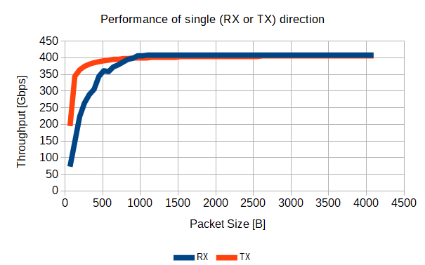
- Ultra-fast DMA module with 400 Gbps throughput based on the PCIe Gen5 x16 or 2x PCIe Gen4 x16 interface.
- Easy to use memory interface for individual reads/writes from/to the card.
- Automatic scripts for complete design synthesis. Run a single make command to create the entire FPGA bitstream.
- Linux kernel driver, DPDK support, user-space library, and tools for configuration.
- Easy custom application creation by user-friendly API for component access and DMA transfers.
User Application
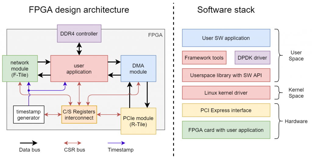
The NDK is designed for creating new network applications with fast packet processing in a deep pipeline. The application core is an area of the FPGA chip dedicated to the user application, which can benefit from the NDK to capture packets from the network interfaces and send data to the host CPU using ultra-fast DMA transfers. The network module (part of the NDK) handles the reception and transmission of network packets. The network module sends the received packets to the application core via the data stream bus (compatible with AXI4-Stream/Avalon-ST). The same data bus is then used to transfer data to the host CPU. The entire NDK is scalable from tens to hundreds of Gbps. It has been designed to send and process multiple packets per clock cycle. The standard data buses of the NDK are optimized to transfer numerous packets at once and thus further scaling the throughput. The mentioned data buses are the MFB (Multi-Frame Bus) and MVB (Multi-Value Bus). In terms of throughput, almost the only limitation is the available FPGA resources.
Many networking applications need large data structures or buffers. Therefore the NDK provides an easy-to-use interface for communication with external memories (typically DRAM). Users can use the interface to rapidly develop a connection tracking table, a flow cache, or data buffers, to provide just a few examples.
The user application implemented in the FPGA can be controlled by read/write requests to an assigned address range. These requests are transmitted from the SW to the application core via a CSR bus compatible with the Intel Avalon-MM. The SW user application can generate these read/write requests through a simple SW API.
Ultra Fast DMA transfers (DMA Medusa IP)
We provide a vendor-independent FPGA architecture and open-source Linux drivers for high-speed DMA transfers using the per-packet approach. The DMA is designed for 400 Gbps throughput and uses multi-channel architecture to support data distribution among CPU cores. The architecture is highly flexible and supports various high-end FPGA families and PCIe bus configurations (up to PCIe Gen5 x16). The DMA IP can utilize more PCI Endpoint blocks to scale throughput to 100, 200, and 400 Gbps.
We have already demonstrated the 400 Gb throughput of the DMA architecture on the Intel Stratix 10 DX Development Kit. However, the same DMA engine can provide a very high throughput also for the Xilinx UltraScale+ and Intel Agilex devices. The NDK Linux driver allows the control of all DMA channels separately. It also provides a user-friendly API to connect your application core directly to the DMA IP. It is also possible to handle DMA transfers through the DPDK driver.
The DMA module IP (DMA Medusa) is not part of the open-source NDK. You can get NDK including DMA Module IP and professional support through our partner BrnoLogic.
Example design
As part of NDK, we provide an example design of a Minimal (reference) application that can be easily extended to provide hardware acceleration for the user application. The example design is built on top of the NDK framework. Due to the well-designed architecture, the Minimal application core comprises only the connection wires necessary to connect network interfaces with the DMA module. Moreover, the Minimal example design includes a unit for data distribution to DMA channels.
Generate bitstream by single command
The primary NDK goal is to provide an easy-to-use framework for the fast development of hardware-accelerated applications and systems. Therefore, we strive to make the steps necessary to build a new bitstream as simple as possible. To start the synthesis process and generate the bitstream, you first need to install a synthesis tool for your FPGA and download the NDK Git repository. Then, you can run the synthesis and generate bitstream by a single command:
# Go to the folder of the example design for the selected card.
$ cd build/your_card/
# Run compilation in the synthesis tool by make command.
$ make
Once the synthesis process is completed, you should have a bitstream file, which can be loaded to the FPGA card using the NDK tools. Alternatively, it is possible to use FPGA programming tools provided by an FPGA vendor.
The example design is built by default for the fastest supported Ethernet standard (for example, 100 GbE or 400 GbE). The NDK usually supports lower speeds as well. If you want to build a bitstream for another Ethernet standard (for example, 10 or 25 GbE), you can specify the speed as the makefile target.
# Run compilation with support for eight 25 GbE channels.
$ make 25g8
The target name (like 25g8) describes the selected Ethernet mode. The number before the letter “g” defines the speed of each Ethernet channel in Gbps. The number after the letter “g” determines the total number of Ethernet channels the FPGA card provides.
Easy to use packet capture solution
The NDK also includes several helpful tools to control the DMA transfers and provide packet capture functionality. One of these tools is used to receive packets from the DMA controller and store them in a PCAP file(s). This tool is called “ndp-receive”. As the example design directly connects Ethernet interfaces and the DMA controller, issuing the “ndp-receive” command captures Ethernet traffic to a PCAP file(s). All NDK tools have a built-in help that will introduce all the options and command line syntax:
$ ndp-receive -h
Usage: ndp-receive [-d path] [-i indexes] [-D dump] [-I interval] [-p packets] [-b bytes] [-B size] [-Rqh]
Common parameters:
   -d path       Path to device [default: /dev/nfb0]
   -i indexes    Queues numbers to use - list or range, e.g. "0-5,7" [default: all]
   -h            Show this text
   -p packets    Stop receiving or transmitting after  packets
   -b bytes      Stop receiving or transmitting after  bytes
   -B size       Read and write packets in bursts of  [default: RX=64, TX=64]
Packet output parameters: (available for one queue only)
   -D dump       Dump packet content to stdout (char, all, header, data)
   -I interval   Sample each Nth packet
Statistic output parameters: (exclusive with -D argument)
   -R            Incremental mode (no counter reset on each output)
   -I interval   Print stats each N secs, 0 = don't print continuous stats [default: 1]
   -q            Quiet mode - don't print stats at end
Receive parameters:
   -f file       Write data to PCAP file  (. for multiple queues)
   -t timestamp  Timestamp source for PCAP packet header: (system, header:X)
                 (X is bit offset in NDP header of 64b timestamp value)
   -r trim       Maximum number of bytes per packet to save
For example, if we want to capture 10,000 packets from all available DMA channels (queues) and store these packets in the PCAP files for each DMA channel separately, we can start the packet capture by a single command:
# Capture 10,000 packets from all DMA channels into the PCAP files.
$ ndp-receive -p 10000 -f my_capture.pcap
The ndp-receive tool stops when the capture of the specified number of packets is completed, and all captured network traffic is stored into PCAP files (the files are named as follows: “my_capture.<index>.pcap” where the <index> is the DMA channel number).
Implement, verify and run
The example design can serve as a source of inspiration when you create your target application. You can easily extend the application core with your acceleration engine or other unique functionality. We provide a documentation of NDK Minimal (reference) application with a detailed description of the application interfaces. You can focus on the application core and utilize NDK to control network interfaces and PCIe with fast DMA transfers.
All network applications need precise verification and testing. Therefore, the NDK provides a UVM verification environment that checks the application’s proper functionality. The verification environment includes a set of Bus Functional Models (BFM) for all application interfaces. All BFMs and the entire verification environment are described in detail in the NDK Minimal App documentation. Once successfully verifying the application core, you can prepare a new FPGA bitstream by a single make command and run the application on the FPGA card.
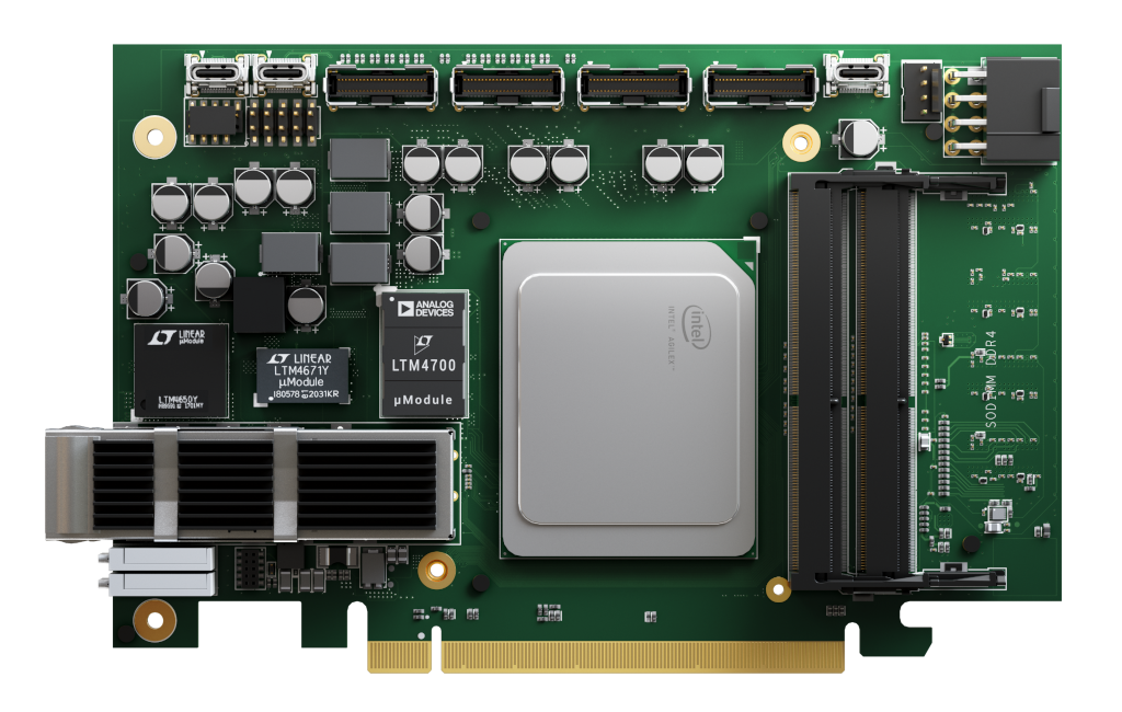
XpressSX AGI-FH400G card by CESNET & REFLEX CES
Supported FPGA cards
The NDK is currently available for several FPGA cards, but it is easily expandable to support any other FPGA-based card with network interfaces and a PCIe connector. We intend to share our source code for all cards to have our code base verified and tested as much as possible. The vast majority of components used in NDK are ready to support a wide range of high-end FPGAs, including Intel Agilex, Intel Stratix 10, Xilinx UltraScale+, and others. If you are interested in the possibility of adding your FPGA card among those supported in NDK, don’t hesitate to get in touch with us. The current list of supported cards can be found on the NDK-APP-Minimal GitHub repository.


